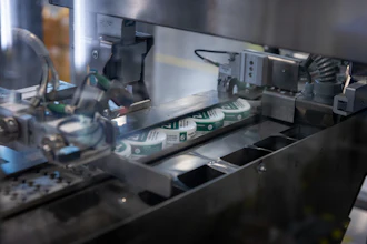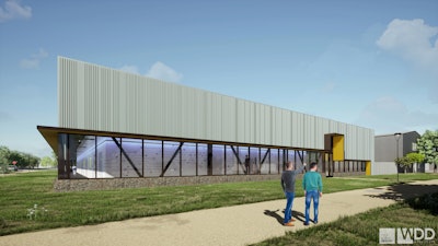
The University of Arkansas began construction on the national Multi-User Silicon Carbide Research and Fabrication Facility, or MUSiC.
Capable of silicon or silicon carbide chip fabrication, this new semiconductor research and fabrication facility will enable the government, businesses of all sizes and universities to prototype in silicon carbide.
This facility will offer low-volume prototyping for high-volume manufacturing, bridging the gap between traditional university research and the needs of private industry. This will accelerate both workforce development and technological advancement in semiconductors by providing a single location where chips can go from developmental research to prototyping, testing and fabrication.
Alan Mantooth, Distinguished Professor of electrical engineering at the U of A, is principal investigator for the MUSiC facility. He stated that with the facility, the university could “begin training the next generation at a variety of degree levels to provide well-trained and educated talent for onshoring semiconductor manufacturing that domestic suppliers offshored in the late 90s and early 2000s. Our training will be equally applicable to silicon and silicon carbide and other materials.”
In addition to the MUSiC facility, the U of A is also home to the first Energy Frontier Research Center in Arkansas, as part of a team of researchers who received $10.35 million from the U.S. Department of Energy.
The Center for Manipulation of Atomic Ordering for Manufacturing Semiconductors is dedicated to investigating the formation of atomic orders in semiconductor alloys and their effects on various physical properties. This research program will enable reliable, cost-effective and transformative manufacturing of semiconductors.
Researchers at the U of A previously established the MonArk NSF Quantum Foundry to accelerate the development of quantum materials and devices. In collaboration with Montana State University, and other member universities, the foundry supports the study of 2-D materials — consisting of a single layer of bonded atoms — by aiding researchers and facilitating the exchange of ideas across academia and industry.
The project leads the fabrication of 2-D material quantum devices and their characterization, using low-temperature electronic transport and optoelectronic techniques.