Toray Engineering Co., Ltd.
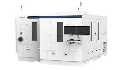
Toray Engineering Co., Ltd. (Tokyo, Japan) announced the UC5000, a high-accuracy semiconductor packaging equipment for panel level packaging (PLP). Sales of the UC5000 began in April.
The UC5000 provides a solution for packaging semiconductor chips on large panels using thermal compression bonding (TCB). It supports panel sizes up to 600mm × 600mm and includes compatibility with glass substrates.
Features:
- Compatible with SEMI Standard panel sizes (515mm × 510mm and 600mm × 600mm)
- Achieves packaging accuracy of ±0.8μm using TCB
- Enables packaging on glass substrates, which are gaining use in PLP
- Includes automatic calibration to maintain accuracy during high-temperature soldering (300°C and above)
- Supports customization to continue functionality from previous models
- Compatible with FOUPs for panels and tape frames, aligning with downstream semiconductor processes
- Developed from technologies with existing mass production track records for small substrates and large panels
The UC5000 meets SEMI Standards and supports high-accuracy semiconductor packaging for applications in AI servers and chiplet-based architectures. It is suitable for use in advanced manufacturing plants seeking large-format PLP solutions.