title
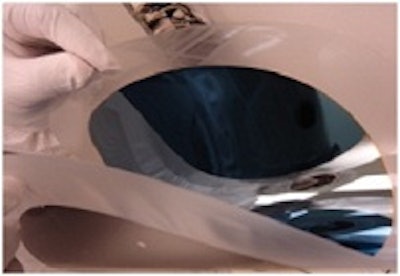
 Dow Corning’s temporary bonding solution for 3D Through-Silicone-Via (TSV) semiconductor packaging is a bi-layer spin-on temporary bonding solutions that eliminates the need for specialized equipment for wafer pretreatment to enable bonding or wafer post-treatment for debonding.
- Process takes less than 15 minutes to complete
- Offers significant potential for reducing the form factor of microelectronic devices targeting next-generation communication devices while improving electrical and thermal performance
- Delivers a uniformly thick adhesive coat and is able to withstand the mechanical, thermal and chemical processes of TSV fabrication
- Debonds the active and carrier wafers without damaging the high-value fabricated devices
- Exhibits a total thickness variation of less than 2 µm for spin-coated films on either 200- or 300-mm wafers
- Exhibits strong chemical stability when exposed to phosphoric acid, nitric acid, organic solvents and other chemicals familiar to TSV fabrication, and both bonding solution and paired wafers show good thermal stability when exposed to the 300°C temperatures common to the TSV process