ARMONK, NY - IBM announced Thursday the first-ever application of applying self-assembling nanotechnology to conventional chip manufacturing to build the next generation computer chips.
The natural “pattern-creating” process that forms seashells and snowflakes has been analyzed by IBM to form trillions of holes which create insulating vacuums around nano-scale wires packed next to each other inside each computer chip.
Researchers have proven that the electrical signals on the chips can flow 35 percent faster, or the chips can consume 15 percent less energy compared to the most advanced chips using conventional techniques.
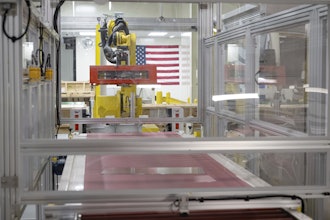
The patented self-assembly process moves a nanotechnology manufacturing method that had shown promise in laboratories into a commercial manufacturing environment for the first time.
The technique causes a vacuum to form between the copper wires on a computer chip, allowing electrical signals to flow faster, while consuming less electrical power. The self-assembly process enables the nano-scale patterning required to form the gaps; this patterning is considerably smaller than current lithographic techniques can achieve.
A vacuum is believed to be the ultimate insulator for what is known as wiring capacitance, which occurs when two conductors extract electrical energy from one another, generating undesirable heat and slowing the speed at which data can move through a chip.


