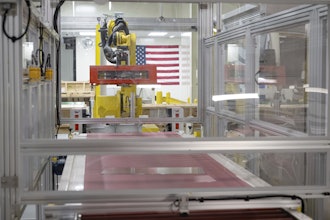
IBM announced Thursday a breakthrough in chip-stacking technology in a manufacturing environment that will allow for a three-dimensional chip layout.
The technology, called “through-silicon vias,” allows different chip components to be packaged much closer together for faster, smaller, and lower-power systems.
The new technology enables the move from horizontal 2-D chip layouts to 3-D chip stacking, eliminating the traditional side-by-side layout on a silicon wafer. The chips can now be stacked on top of one another, resulting in a compact layout of components that will reduce the size of the overall chip package and boost data flow speed.
This stacking method will eliminate the need for long metal wires that connect 2-D chips currently. By using the through-silicon vias, the vertical connections are etched through the silicon wafer and filled with metal.
IBM is currently running chips using the through-silicon via technology in its manufacturing line and will begin making sample chips method available to customers in the second half of 2007, with production in 2008.
The first application of this through-silicon via technology will be in wireless communications chips that will go into power amplifiers for wireless LAN and cellular applications.


