 Sri Peruvemba
 In the rapidly-paced world of consumer electronic products, silver nanowire material offers uniquely valuable properties to a range of mass-produced touch screens for consumer products, OLED lighting components and solar collection cells. Specifically, silver nanowire's key manufacturing values are its clear production advantages versus traditional materials used in those three major product areas. The material also trumps legacy conductor materials in end-product performance.
Three-fold Economies
Manufacturing efficiencies relevant to silver nanowire as a replacement material includes reduced capital equipment costs, notably faster processing speed and reduced energy requirements. Additionally, availability of raw materials, reduced material requirements and ease of assembly also contribute to this material's increasing adoption across several industries.
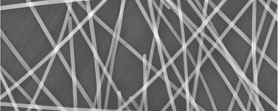
Rarely have the obvious intrinsic values of technology breakthroughs been more clearly defined. In the realm of transparent electrodes used for touchscreen displays, organic light-emitting diode (OLED) lighting, there is a massive switch on from the incumbent material, indium tin oxide (ITO) to electrodes based on silver nanowires (AgNW). This transition in display technologies, particularly where display or touch screen flexibility, weight, and manufacturing efficiencies are required, is due to several easily understood differences between the two materials.
For example, consumer product creators demand conductivity below 100Ω/square to make their touchscreens more responsive and further improve the user experience. Silver is the most conductive material in use. For large area touchscreens like 20-inch monitors, higher conductivity is essential for a fast response time and to detect 10-finger touch. In laptops and smartphones, film-based transparent conductors can create thinner, lighter and stronger touchscreens. Higher transmission also enhances battery-life-per-charge and creates brighter displays since the AgNW-based touch sensor does not impede light as greatly as traditional materials.
The material, already being used in a significant number of consumer and industrial products, offers lower manufacturing and per-unit product costs and enables far easier scaling. Roll-to-roll processed silver nanowire transparent conductors are the clear choice especially for new production facilities needing high throughput and easier processing. They're also on target for OEMs needing a thin, light, flexible material delivering high performance for their next killer product.
Transparent conductors may also be applied as electrodes for LCD, OLED, thin film photovoltaic cells and applications not yet imagined. In general, the design requirements remain the same: higher conductivity and improved light transmission.
AgNW/ITO Comparisons
Single-layer touch sensors based on silver nanowires offer notably lower cost than ITO because they use fewer layers of material in the touchscreen stack. This equates directly to dramatically reduced manufacturing complexity and reduced materials consumption. Single layer sensors can be made with silver nanowires that eliminate the need for an additional substrate and adhesive. This enables thinner CE product displays. Thin is in because nearly all products, particularly in the consumer electronics domain need to be sleek and aesthetically pleasing.
If slim industrial design is a must, the next trend is flexibility. In bending tests, silver nanowire coated films withstand greater than 450,000 turns around a 1mm bending radius, demonstrating great fit in flexible, rollable electronic products. ITO being a ceramic material, is brittle and does not flex.
Addressing Environmental Concerns
When compared directly, silver nanowire-based touchscreens range from slightly less to significantly lower in cost than equivalent ITO film-based solutions. Silver nanowires are made using equipment that are about a tenth the cost of ITO manufacturing equipment. Silver nanowires can also be patterned using room temperature lasers. Laser patterning equipment costs are also lower. Further, the manufacturing processes require no consumables. Additionally there are no hazardous waste disposal problems. It’s a greener way of making products.
Silver nanowire production is a clean, automated process with low labor costs and fairly limited space requirements. Production can be quickly scaled to meet demand from giant CE product OEMs.
Major touch screen players are already catching on to silver nanowires' manufacturing and product performance advantages. These include leading industry heavyweights like Hitachi, LG, Nissha, Okura, Samsung, TPK, 3M, and many other manufacturing giants. OEMs like DELL, Lenovo, HP, and Toshiba have already shipped and continue to launch their latest CE products using silver nanowire touch screens.
For manufacturing engineers focusing on improved yield, processing speed, material consumption and overall cost reduction in touch displays, OLED lighting products, solar collector arrays and other products, silver nanowire-based processing offers immediate advantages. Manufacturing with silver nanowire-based technology doesn't have a downside. Its advantages are numerous. The material is cost-effectively accelerating the transition to products we used to only imagine.
Sri Peruvemba is vice president at Cambrios Technologies Corp.