Because many high-volume printed circuit assemblies are sent outside the United States, it is challenging to test the lower volume/high turnover assemblies domestically. But this does not need to be a problem — some simple planning and the right contract manufacturer (CM) can solve this issue.
The challenge is that the US market is made up of high-technology/low production quantity assemblies. In many circuit bed of nails cases, test is not an option because of development time, cost and the difficulty associated with finding a place for a 30-40 mil test point. These same test points also create significant EMI concerns for most electrical engineers. The challenge is to find a way to thoroughly test a fully populated circuit in a timely, cost-effective way without compromising signal integrity.
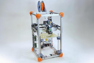
Depending on the technology, the challenge can be as simple as making minor design changes that can happen at the gerber level to requiring a significant revision to the board in question. First let’s conquer the simple. For analog, RF and lower technology digital boards the approach is the simplest. Typically, straightforward flying probe test is the answer. The better EMS companies use a dual-sided flying probe tester. For this test approach, the test engineer simply asks that the vias not be covered with soldermask, which can be a simple change handled at the CAM/gerber level. Depending on the test coverage, the test department may recommend adding vias, assuming your design can handle it from an electrical perspective. If, as in sensitive analogs or RF technology boards, vias are being avoided the tester may be able to test at the solder joint. Allowing this requires customers to be open minded about “witness marks” left behind by the tester. Harder solder – for example lead-free –reduces this problem. Testing this technology typically results in some of the higher test coverage approaching 100 percent.
High-technology product can create more of a challenge. The technology in this class includes high-speed digital, via in pad, blind buried vias and high BGA count. The unknown in this case is the number of circuits that actually never see an external via, making it impossible to probe the circuit. The previous guidance still applies: have a via exposed for every circuit. This includes making sure they are not covered by a component or soldermask. Typically, this results in adequate test coverage, but no one wants to be just okay.
To continue reading the full article, click here to visit our partner publication, PD&D.